
PCB拼板设计规范

Printed Circuit Boards (PCBs) are an essential component of almost every electronic device. PCBs are used to connect electronic components and create circuitry. PCB assembly is the process of combining multiple PCBs together to form a complete electronic device. PCB assembly is a complex process that requires careful planning and attention to detail. In this article, we will look at the PCB assembly process and provide some guidelines for designing PCBs for assembly.
PCB Design Guidelines for Assembly
Before designing the PCB, it is important to consider the assembly process. Failure to consider the assembly process can result in costly mistakes and wasted time. The following are some guidelines to consider when designing a PCB for assembly:
1. Panelization
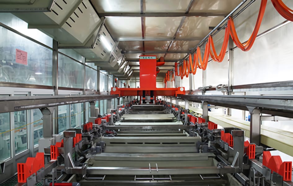
Panelization is the process of combining multiple PCBs together on a single panel. Panelization can help to reduce the cost of the PCB assembly process. When designing the PCB, it is important to consider the panelization process and design the board so that it can be easily panelized.
2. Component Placement
Component placement is an important part of PCB design. Components should be placed in such a way that they can be easily assembled. The following are some guidelines for component placement:
– Components should be placed on one side of the board.
– Components should be placed in a logical order so that they are easy to find during assembly.
– Components should be placed so that they do not interfere with other components.
3. Component Spacing
Component spacing is also an important part of PCB design. Components should be spaced far enough apart to allow for easy assembly. The following are some guidelines for component spacing:
– Components should be spaced at least 0.025 inches apart.
– Components should be spaced far enough apart to allow for easy access during assembly.
– Components that generate heat should be spaced far enough apart to allow for adequate airflow.
4. Trace Width and Spacing
Trace width and spacing are important considerations in PCB design. The following are some guidelines for trace width and spacing:
– Trace width should be at least 0.010 inches.
– Trace spacing should be at least 0.010 inches.
– Trace widths should be adjusted to accommodate higher current levels.
5. Solder Mask
Solder mask is a protective layer that is applied to the PCB to prevent solder from adhering to areas of the board where it is not intended. The following are some guidelines for solder mask:
– Solder mask should cover all areas of the board where solder is not intended.
– Solder mask should be applied evenly to avoid excess thickness.
– Solder mask should be applied in a way that does not interfere with the assembly process.
6. Silkscreen
The silkscreen is a layer on the PCB that contains information about the board, such as component values and part numbers. The following are some guidelines for the silkscreen:
– The silkscreen should be legible and easy to read.
– The silkscreen should be placed in a location that does not interfere with the assembly process.
– The silkscreen should not be used to convey critical information, such as component polarity.
Conclusion
Designing PCBs for assembly is a complex process that requires careful planning and attention to detail. Failure to consider the assembly process can result in costly mistakes and wasted time. The guidelines outlined in this article are intended to help designers create PCBs that are easy to assemble and result in high-quality products. When designing a PCB for assembly, it is important to work closely with the manufacturer to ensure that the design meets their specifications and requirements. By following these guidelines, designers can create PCBs that are easy to assemble and result in high-quality electronic products.
 3002788751